The U.S. Department of Energy unveiled plans to build two GPU-accelerated leadership class supercomputers (Summit at ORNL and Sierra at LLNL) in a combined $325M USD procurement to be installed in 2017 that will be based on next-generation IBM POWER servers incorporating NVIDIA® Volta GPU accelerators plus NVLink™ high-speed GPU interconnect technology. The announcement by U.S. Secretary of Energy Ernest Moniz fixed 2017 delivery dates for both Volta GPUs and NVlink connectivity to IBM Power processors.
In addition, Secretary Moniz also announced approximately $100 million to further develop extreme scale supercomputing technologies as part of a research and development program titled FastForward2. The FastForward2 funding seeks to develop critical technologies needed to deliver next-generation capabilities that will enable affordable and energy-efficient advanced extreme scale computing research and development for the next decade. The joint project between DOE Office of Science and National Nuclear Security Administration (NNSA) will be led by computing industry leaders AMD, Cray, IBM, Intel and NVIDIA.

Secretary Moniz (courtesy DOE)
The “Summit” system at Oak Ridge National Laboratory will be capable of delivering 150 to 300 peak petaflops, and be used for open science. The smaller (relative to Summit) Sierra system will deliver performance well in excess of 100 peak petaflops as a key element of Lawrence Livermore National Laboratory’s national nuclear security mission. (NNSA also procured the Intel KNL powered LANL Trinity supercomputer to be delivered in 2015.) The two GPU powered systems will be considerably faster than the U.S.’s current speed champ, Oak Ridge’s “Titan,” which delivers 27 peak petaflops, as well as the world’s fastest, Tianhe-2 at China’s National Super Computer Center, in Guangzhou, which delivers 55 peak petaflops.
The risks inside the 2017 delivery date
The 2017 date gives the NVIDIA and IBM partnership time to finish the silicon implementations of both the Volta GPUs and NVlink on-chip interconnect. As such, these two announcements represent considerable risk for NVIDIA and IBM as Volta includes stacked DRAM (an untried technology in GPUs and in systems approaching exascale) plus NVlink which is only running in simulation – not silicon – at the moment.
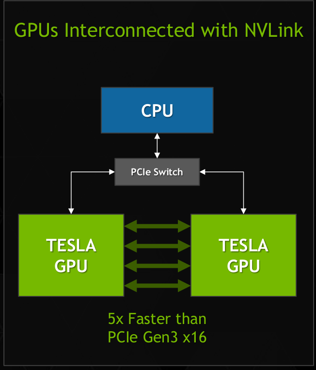
NVlink (courtesy NVIDIA)

SIMULATED NVlink speedups (courtesy NVIDIA)
According to NVIDIA, Volta™ will deliver considerably higher performance than the company’s current Maxwell™ architecture and subsequent Pascal™ design. Delivering significantly higher levels of computational performance than anything available today, NVIDIA Volta GPUs will provide Summit and Sierra with more than 90 percent of the peak floating point processing.
It is unclear from the announcements but it seems likely that the Volta GPUs will incorporate stacked DRAM for these two procurements. Stacked memory technology promises to eliminate (or significantly reduce) memory-bandwidth limitations for many applications by providing approximately 1 TB per second of memory bandwidth. We do not yet know the random access behavior, but stacked DRAM seems a likely candidate to better support sparse matrix operations. (Click this hyperlink to see that stacked DRAM is specifically called out on the NVIDIA roadmap for Volta.)

NVlink and stacked memory (image courtesy NVIDIA)
The $325M investment and reliance on GPUs for 90% of the machine performance sends a clear message to the HPC community – GPU accelerators are now a core technology rather than an add-on. A failure of either the untried Volta or NVlink technology would represent a significant, perhaps mortal blow to the NVIDIA exascale aspirations and significantly impact the ability of the Summit and Sierra machines to support their missions.
However, we have seen NVIDA perform a remarkable penetration into HPC over the past few years through the creation of CUDA (a roughly billion dollar investment according to NVIDIA CEO Jen-Hsun) and a remarkably agile silicon design effort.

NVIDIA growth as of 2012 (courtesy NVIDIA)
We have been reporting the penetration of GPU computing into the enterprise space as well as HPC. For example, our SC14 special edition article for Scientific Computing, Today’s Enterprising GPUs, looks at commercial GPU-computing success stories such as Shazam, Baidu (China’s biggest search engine), Yanix (Russia’s biggest search engine), and various machine-vision and animation companies where rows of GPU powered servers are busily humming away making money:
“So, who are the winners who have staked their claims and are capitalizing on rows of GPU-accelerated servers that are busily humming away making money? First, think of companies with business models that require lots of computing capability without having to move outlandish amounts of data. Such organizations fit within the current sweet spot in the GPU technology landscape of lots of computational capability for not much (a) investment and (b) power consumption relative to CPU implementations.”
Next, think of organizations that do need to move outlandish amounts of data. Such organizations fit within two rough categories:
1. those that process large amounts of data, but where the profit-based activity is still “relatively” low-bandwidth (e.g. like a search model)
2. those where both the processing and profit are high-bandwidth
As always, the beyond-the-bleeding-edge HPC market for leadership class systems represents an opportunity to prove new technology and potentially fail from even the smallest of details. The joke “how do you make a small fortune in HPC … start with a large one!” applies.
Working with brand-new and very dense memory systems plus very tightly packed register files and caches on the GPU and the new NVlink protocol raises concerns over “silent errors” where multi-bit errors silently bypass the ECC memory protections. With tens of thousands of GPUs each containing many SMX processors plus multiple, asynchronous cache and shared memory transactions constantly happening in a dynamic clock environment, even statistically improbable (for small number of GPUs) double-bit “silent errors” can happen at scale to introduce non-physical artifacts that could potentially be devastating when considering questions of nuclear stockpile stewardship and other physical simulations. With 3D packing of the memory chips, could a single cosmic ray trigger a silent error? Similarly, how does temperature, humidity, age, and other factors affect the hardware?
NVIDIA’s Sumit Gupta graciously answered our questions at SC14 on this issue as follows, “NVIDIA does not release error rate information. However, the two large procurement by the DOE illustrate their confidence in NVIDIA technology”.

NVIDIA’s Sumit Gupta, General Manager, Tesla Accelerated Computing Business. (courtesy NVIDIA)
Of course, we are all waiting to get our hands on NVIDIA Volta GPUs and investigate the potential of NVlink! Sign us up for early testing!
Leave a Reply